Big Maxwell GM2*0
Message boards :
Graphics cards (GPUs) :
Big Maxwell GM2*0
Message board moderation
| Author | Message |
|---|---|
|
Send message Joined: 25 Sep 13 Posts: 293 Credit: 1,897,601,978 RAC: 0 Level Scientific publications |
http://wccftech.com/article/generation-graphics-prospects-nvidia-big-daddy-maxwell-16ff-ports/ 3072 CUDA cores/24 SMM/1.1GHz base reference clock? A larger L2 cache (3MB) with same 1/1 core/L2 ratio as GTX980. If a DP64 1/4 ratio (8 per 32c block @ 32per SMM) equals 768 DP64. At 1/2 ratio (16 per 32c block @ 64 per SMM) a monster 1536DP64 cores. I'm guessing 1/4 DP core ratio. If clocks are high enough this will equal GK110 960DP64 @ 1.1-1.7 teraflops of Double precision. Here are some early numbers http://www.sisoftware.eu/rank2011d/show_run.php?q=c2ffccfddbbadbe6deeadbeedbfd8fb282a4c1a499a98ffcc1f9&l=en |
|
Send message Joined: 17 Aug 08 Posts: 2705 Credit: 1,311,122,549 RAC: 0 Level Scientific publications |
the 1st article wrote: The GK110 is roughly 550mm^2 and the limit of TSMC is at roughly 600mm^2. So can the GM200 exist on a 28nm Node? Absolutely, yes. Will it? Well, the consumer samples taped out a long time back, and they are sure as hell not on 16nm FinFET. Which makes sense to me. I edited the title, so that it doesn't imply GM2x0 would be made in 16nm FinFET tech. MrS Scanning for our furry friends since Jan 2002 |
|
Send message Joined: 25 Sep 13 Posts: 293 Credit: 1,897,601,978 RAC: 0 Level Scientific publications |
http://devblogs.nvidia.com/parallelforall/increase-performance-gpu-boost-k80-autoboost/ For the Dual Administer: C.C 3.7 [?] (Larger Register(s) / More shared memory @ 128Kb per) Third GK*10 revision >>> GK210 Dual Tesla Board build upon 300TDP with 4992 Total CUDA cores (2496c/13SMX per Board/150TDP) Revamped GPU boost: "Using NVML your CUDA application can choose the best GPU Boost setting without any user intervention. Even when the applications clocks permission setting prevents your app from changing the application clocks, NVML can help you inform application users about this so they can consult with their system administrator to enable GPU Boost. To achieve exactly this the popular GPU-accelerated Molecular Dynamic application GROMACS will use NVML in its next release to control GPUBoost on NVIDIA® Tesla® accelerators." For Tesla > GRID > Quadro: GPU Deployment Kit includes NVIDIA Management Library (NVML) K80 lights 832 DP64 cores per Board [1664 Total DP64] From look of GK210 SMX: the Polymorph Engine non-functional (Not on Die) 16 TMU per SMX (same ratio as C.C 3.0/3.5) GK210: 4992 CUDA [300TDP_26SMX] [13] 192c SMX per board [26] Total SMX at 300 Total TDP @ 11.538 watts per SMX @ 0.060 w per core Lower Power Operating Points than GM204 or GK110B revision. Inclusion (Polymorph Engine inside SMM/SMX) See Maxwell now thread. Future GM2*0: 3072 CUDA [250TDP(?)_24SMM] [24] 128c SMM @ 12.5 watts per @ 0.081 watt per core |
|
Send message Joined: 17 Aug 08 Posts: 2705 Credit: 1,311,122,549 RAC: 0 Level Scientific publications |
Lower Power Operating Points than GM204 or GK110B revision. If you ran GM204 at 550 - 850 MHz with appropriate voltage it would easily beat GK210's power efficiency. MrS Scanning for our furry friends since Jan 2002 |
|
Send message Joined: 25 Sep 13 Posts: 293 Credit: 1,897,601,978 RAC: 0 Level Scientific publications |
If you ran GM204 at GK210 clocks: GM204 single is less than GK210 Double Flops. Once Big Maxwell specs are confirmed- this could be only full compute worthy Titan Maxwell (dual card also) until late 2016 early 2017 Pascal arch. I won't include a Maxwell GM204 SMM in same category as Kelper arch. All compute Kepler SMX includes as many DP64 cores in one SMX as whole GM204 die(64). Titan brand sold a lot of enabled GK110. Excluding Tesla and Quadro for 64bit- a Titan work's in most areas. The Titan DP64 driver setting lowers core clocks to ~600 MHz or so at lower voltage than clocks for Single Precision. |
|
Send message Joined: 17 Aug 08 Posts: 2705 Credit: 1,311,122,549 RAC: 0 Level Scientific publications |
If you ran GM204 at GK210 clocks: GM204 single is less than GK210 Double Flops. What?! GK210 runs DP at 1/3 its SP performance, so it's equivalent to 2880/3 = 960 shaders. GM204 has 2048 shaders for SP, which actually perform more like 1.4*2048 = 2867 Kepler-Shaders. At similar clocks GM204 SP would be about 3 times as fast as GK210 DP. Any why are you talking about DP anyway? If you need DP and nVidia you're badly f*cked anyway, because nothing below an ultra-expensive Titan makes any sense. the amount of DP cores in gaming Maxwell doesn't matter, because performance would s*ck anyway. It's meant for compatibility, testing and debug, but not for pure number crunching. I know people are not aware of this and like to run Milkyway on nVidia cards, but that doesn't change the fact that DP-crunching on either Kepler or Maxwell, or mainstrea-Fermi for that matter, is a pretty bad idea. MrS Scanning for our furry friends since Jan 2002 |
|
Send message Joined: 25 Sep 13 Posts: 293 Credit: 1,897,601,978 RAC: 0 Level Scientific publications |
CUDA7 (pre-production release) will be here around the new year. Production release near April. (NVidia last couple Major CUDA releases have been early in the year) Current CUDA driver is 6.5.30 For the upcoming release of GM2*0 Titan and GTX 960: here is the current (as) list prices for Kelper and Maxwell on Newegg with each board having a per core cost. Factoring in power costs for DC FP32 (ACEMD)--- Lower sustainable operating prices for GM204/107 efficiency as cost to purchase higher initially. GM204/GK110/GK104/GM107/GK106 board's power consumption varies [-30>+20%] with a sustained OP: each board creates unique traits- managing complex currents. [list=] 250W TDP 2880 core Titan Black @ 1000usd @ 34.7 cents per core (960 Total DP/64 DP SMX enabled) 375W TDP 5760 core Titan-Z @ 1500usd @ 26c per core (1920Total DP/64 DP SMX enabled) 300W TDP 3072 core [refurished] GTX 690 @ 519 @ 16.9c per core ( 128Total DP/8DP core per SMX) 250W TDP 2880 core [refurished] GTX 780ti @ 419 @ 14.5c per core ( disabled 64DP SMX- driver enables 8 per SMX for 120 total DP) 225W TDP 2304 core [refurished] GTX 780 @ 319 @ 13.9c per core ( disabled 64DP SMX- driver enables 8 per SMX for 96 Total DP) 165W TDP 2048 core GTX 980 @ 549 @ 26.8c per core ( 64 Total DP64 core/ 4 per SMM) 145W TDP 1664 core GTX 970 @ 329 @ 19.7c per core ( 52 Total DP64 core/ 4 per SMM) 230W TDP 1536 core [refurished] GTX 770 @ 239 @ 15.5c per core ( 64 Total DP/ 8 per SMX) 195W TDP 1536 core [refurished] GTX 680 @ 229 @ 14.9c per core ( 64 Total DP/ 8 per SMX) 170W TDP 1344 core [refurished] GTX 670 @ 179 @ 13.3c per core ( 56 Total DP) 140W TDP 1344 core [refurished] GTX 660ti @ 159 @ 11.8c per core (56 Total DP) 170W TDP 1152 core [refurished] GTX760 @ 159 @ 13.8c per core (48 Total DP) 140W TDP 960 core GTX660 @ 134 @ 13.9c per core (40 Total DP) 110W TDP 768 core [refurished] GTX650ti @ 89 @ 11.5c per core (32 Total DP) 60W TDP 640 core GTX 750ti @ 129 @ 20.1c per core (20 Total DP) 55W TDP 512 core GTX 750 @ 109 @ 21.2c per core (16 Total DP) 25W TDP 384 core GT 630 @ 37 @ 9.4c per core (16 Total DP) [/list] C.C 5.2 Maxwell per core cost around 23cents- while Kepler C.C 3.0 much lower. C.C 5.0 per core cost higher than Non-DP enabled 3.5 C.C boards. Notice the GTX 980 per core cost same as Titan-Z. 1 GTX 970/980 offers GPUGRID best cost/runtime/power usage. Multiple GM107 boards are also a good choice. (this could change with GTX960 release and Maxwell's Titan purchase price) Kelper GTX 660ti and GTX780(ti) show to be decent cost/power/runtime; depending upon silicon lottery for eco-tuning. Numerous choices exist from the eco-tune point of view. Outside of GPUGRID- C.C 3.5 still a more complete compute arch. A OpenCL AMD Tahiti (2048/1792Total cores[512/448 DP64c]) is currently priced around 11cents per core. CUDA's DP accuracy different than OpenCL. Have a look at Math Libraries for each and see which you'd rather trust for long runtime compute. |
 Retvari Zoltan Retvari ZoltanSend message Joined: 20 Jan 09 Posts: 2380 Credit: 16,897,957,044 RAC: 0 Level Scientific publications |
                              price | price    | Total
                                USD | per core |   DP
250W TDP 2880 core Titan Black 1000 | 34.7c    |  960 (64 DP SMX enabled)
375W TDP 5760 core Titan-Z     1500 | 26c      | 1920 (64 DP SMX enabled)
300W TDP 3072 core GTX 690*     519 | 16.9c    |  128 (8DP core per SMX)
250W TDP 2880 core GTX 780ti*   419 | 14.5c    |  120 (disabled 64DP SMX- driver enables 8 per SMX)
225W TDP 2304 core GTX 780*     319 | 13.9c    |   96 (disabled 64DP SMX- driver enables 8 per SMX)
165W TDP 2048 core GTX 980      549 | 26.8c    |   64 (4 per SMM)
145W TDP 1664 core GTX 970      329 | 19.7c    |   52 (4 per SMM)
230W TDP 1536 core GTX 770*     239 | 15.5c    |   64 (8 per SMX)
195W TDP 1536 core GTX 680*     229 | 14.9c    |   64 (8 per SMX)
170W TDP 1344 core GTX 670*     179 | 13.3c    |   56 (8 per SMX)
140W TDP 1344 core GTX 660ti*   159 | 11.8c    |   56 (8 per SMX)
170W TDP 1152 core GTX 760*     159 | 13.8c    |   48 (8 per SMX)
140W TDP  960 core GTX 660      134 | 13.9c    |   40 (8 per SMX)
110W TDP  768 core GTX 650ti*    89 | 11.5c    |   32 (8 per SMX)
 60W TDP  640 core GTX 750ti    129 | 20.1c    |   20
 55W TDP  512 core GTX 750      109 | 21.2c    |   16
 25W TDP  384 core  GT 630       37 |  9.4c    |   16
*=refurbished
I've just made your spreadsheet more readable. |
|
Send message Joined: 25 Sep 13 Posts: 293 Credit: 1,897,601,978 RAC: 0 Level Scientific publications |
I've just made your spreadsheet more readable. Gentlemanly of you For all those spreadsheet programs available: MS notepad doesn't organize! |
|
Send message Joined: 7 Jun 12 Posts: 112 Credit: 1,140,895,172 RAC: 0 Level Scientific publications |
http://www.chiploco.com/nvidia-geforce-gtx-titan-ii-3072-cores-12gb-memory-36760/ 8gb memory is more likely, 12 gb is too much for only 3072 cuda cores gtx 980 2048 cuda cores and 4 gb ram So the new titan Z will have about 6000 cuda cores and maybe 16gb ram..? And another BAD news http://wccftech.com/amd-nvidia-20nm-16nm-delayed/#ixzz3MvZ5AzSg Again.. So also in the segment of video cards coming here CPU scenarios" monopoly.. |
|
Send message Joined: 7 Jun 12 Posts: 112 Credit: 1,140,895,172 RAC: 0 Level Scientific publications |
http://www.tweaktown.com/news/42269/amd-nvidias-next-gen-gpus-delayed-supply-constraints-blamed/index.html I think it's a scam, agreed between Apple and NVIDIA. Everyone has to help in gain money .. unfortunately, my group can not harm these companies .. and also this project do not mind and action nvidia commons will not fall .. |
skgiven Send message Joined: 23 Apr 09 Posts: 3968 Credit: 1,995,359,260 RAC: 0 Level Scientific publications |
http://www.tweaktown.com/news/42269/amd-nvidias-next-gen-gpus-delayed-supply-constraints-blamed/index.html There is a typo in that report, they said Apple instead of AMD; "so that leaves Apple and NVIDIA with a very limited supply of 20nm dies". Basically TSMC will be busy making 20nm Qualcomm SoC's, so NVidia and AMD will have to wait their turn. This isn't such a bad thing - AMD and NVidia need bigger dies. That means TSMC will have refined the process by the time its AMD and NVidia's turn. FAQ's HOW TO: - Opt out of Beta Tests - Ask for Help |
|
Send message Joined: 25 Sep 13 Posts: 293 Credit: 1,897,601,978 RAC: 0 Level Scientific publications |
http://wccftech.com/nvidia-planning-ditch-maxwell-gpus-hpc-purposes-due-lack-dp-hardware-update-tesla-line-pascal-2016-volta-arriving-2017/ Once Big Maxwell specs are confirmed- this could be only full compute worthy Titan Maxwell (dual card also) until late 2016 early 2017 Pascal arch. Kelper's HPC boards will reign until late 2016/early 2017 due to Maxwell's weak DP core structure (1 DP core in every 32c subset block and no 64bit/8byte banks like Kelper) The GeForce Titan Maxwell (4 DP per 32c subset/32DP per SMM) will be the full feature compute Maxwell with less DP cores (768) compared to Kelper's 960/896/832 DP64 line-up unless GM2*0 has 64DP for every SMM (1/2ratio) This will keep Titan prices higher unless AMD 2015 offering +20% GM2*0. The GTX 960(ti) will feature [3] different dies. (8SMM/10SMM/12SMM) The 8SMM could be 70-100TDP with Ti variants being 100-130TDP. |
|
Send message Joined: 17 Aug 08 Posts: 2705 Credit: 1,311,122,549 RAC: 0 Level Scientific publications |
@eXaPower: let's wait and see, so far we've only got rumors (although lot's of it). I'm sure the biggest Maxwell chip will be better at DP than GK210. The market and profit margin for such chips in the form of Teslas and Quadros is just too large for nVidia to ignore. For gaming they could just as well give us 2 GM204 on one card instead of creating a new flag ship chip. And don't forget the higher efficiency of Maxwell per shader - some of this will also apply to DP once there are a lot of DP-capable shaders. And you actually don't need separate shaders for SP and DP. I really don't understand why nVidia is doing this since big Kepler. There's surely a slight improvement in power efficiency, which the gaming cards gladly take. The DP shaders don't cost them much area/transistors, because there so few of them. But for the big chips providing plenty of DP shaders really costs a lot of area/transistors. So before nVidia chooses to outfit their new very power- and area-efficient flagship with too few DP units, they should rather sacrifice a little power efficiency and use combined shaders, where 2 or 4 SP units work together as 1 DP unit. @Jozef: this is not a scam. TSMCs planar 20 nm process provides little power consumption and transistor performance benefits over 28 nm at hardly reduced cost per transistor. It only makes sense to use this process for chips with large win margins (Apple, TSMC flag ship chips to a lesser extent) and where every mW of power saved counts (mobile). Sure, power also counts for desktop GPUs, but it's not like Maxwell is doing badly. And TSMCs 20 nm capacity is still very limited, so it's first used for who ever pays the most (probably Apple). Since it's a new process the yields are very probably also not good yet, which is OK for small chips (mobile SoCs), but prohibitive for monster GPUs. It may look like a conspiracy, but it's really just economics - these guys need to make money, and they'll simply take the actions they think are best suited for this purpose. If they stagnate for too long someone else will take over their market. MrS Scanning for our furry friends since Jan 2002 |
|
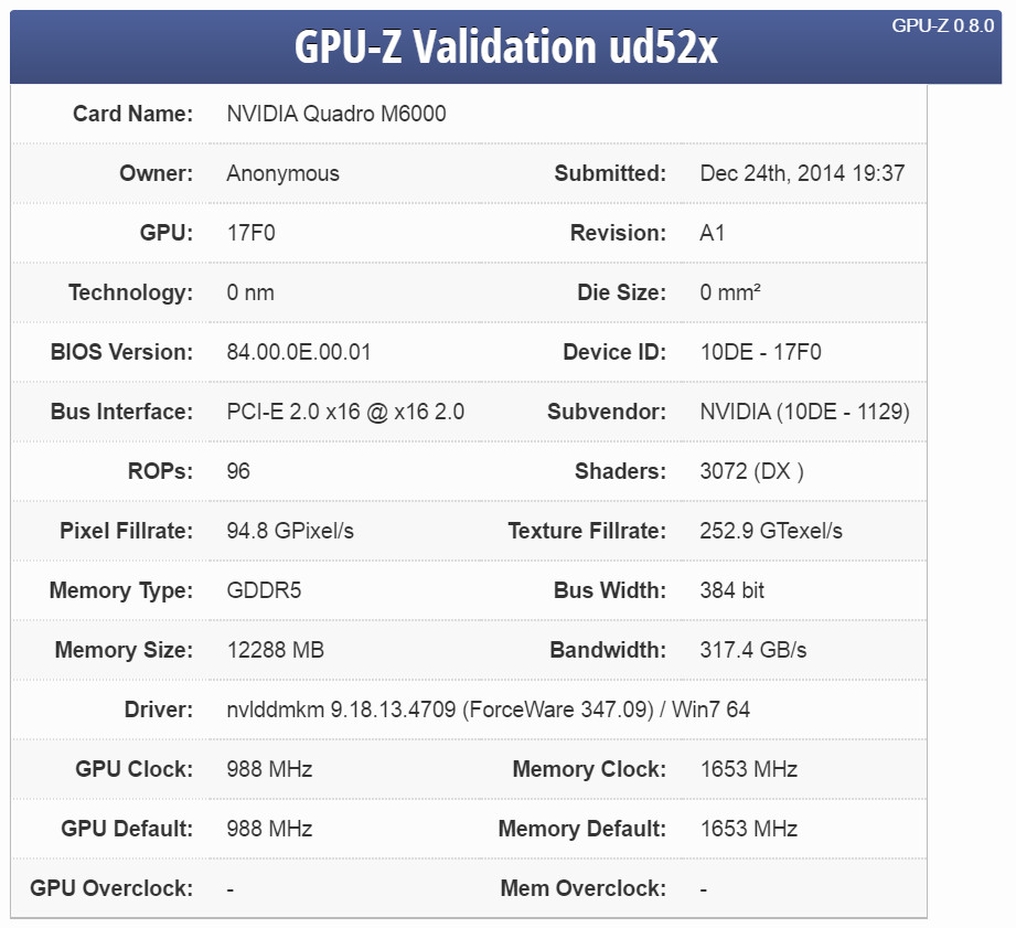
Send message Joined: 25 Sep 13 Posts: 293 Credit: 1,897,601,978 RAC: 0 Level Scientific publications |
A GM200 Quadro been spotted in GPU-Z database: 3072CUDA/192?256?TMU/96ROPS. If "M6000" is indeed the replacement for K6000 than DP performance will be near 1.7 Teraflops. A forth coming announcement will be this month. (Could include a CUDA7 toolkit) As for a Dual GM204 dropping: this could happen after AMD releases their 390 series. (I hope AMD top card is very strong and +20-30% GM204 to force NVidias hand) A specialty Dual GM204 might be released by Asus or someone- similar to ROG Mars GTX 760. Maybe the GTX 960ti is a Dual GPU candidate also? Remember: the very successful GTX690 (June2012) was released when Tahiti and GK104 were battling for top spot until Feb 2013 when the Titan became the Flagship with GTX 780 being a stop gap. (May2013) The hot and power hungry reference Hawaii released with weaker DP than the very successful Tahiti. ( AMD best arch and an excellent card for OpenCL compute) Nvidia came back with GTX780ti. Nvidia ruled the roast during 2014 with long in tooth Kelper and low-Mid range 512/640 Maxwell for the first half of 2014 and very strong gaming GM204 for second half. (AMD x295 success forced Nvidia to slash Titan-Z price in half) AMD cards are no where original release prices unlike NVidia who's premium price is worth it to some- due to Nvidia's Developer Program offering chock full of goodies for Linux and Windows) |
|
skgiven Send message Joined: 23 Apr 09 Posts: 3968 Credit: 1,995,359,260 RAC: 0 Level Scientific publications |
 0nm is smaller than expected ;p Aside from the likely 'app cant read' oddities (which might suggest 20nm; though unlikely IMO), it looks reasonably plausible, though 6600MHz is a little strange (possibly Eco tuned 7GHz GDDR5). The bit that makes no sense is the PCIE2 board, but it didn't the last time I saw a GPU ES. This raises the question of 20nm, 16nm and thus release dates; I really didn't expect a 20nm anything from NV any time soon, and I still don't... As for a GTX990, while I might be wrong, I totally expect this. A 300W TDP is likely and it might match a GTX Titan Z in terms of throughput performance for here but be >20% more power economically and a LOT cheaper to buy... FAQ's HOW TO: - Opt out of Beta Tests - Ask for Help |
|
Send message Joined: 17 Aug 08 Posts: 2705 Credit: 1,311,122,549 RAC: 0 Level Scientific publications |
0nm is smaller than expected ;p Ouch - there are going to be some serious short channel effects with such small structures! I heard the chip is going to be called Atom, but they're still fighting with Intel in court over it. MrS Scanning for our furry friends since Jan 2002 |
|
Send message Joined: 25 Sep 13 Posts: 293 Credit: 1,897,601,978 RAC: 0 Level Scientific publications |
This raises the question of 20nm, 16nm and thus release dates; I really didn't expect a 20nm anything from NV any time soon, and I still don't... You're right- Nvidia will be 16FinFet. Speculation: The first batch of GM200 is likely 28nm unless TSMC has an excellent recipe of being extremely silent with mis-information spread and 16nm yield is way above initial expectations. 20nm is for low power SOC (phones) and maybe ~75TDP AMD APU's. AMD could stay at 28nm and then go Global Foundries 14nm. We might be stuck at 28nm until next year. (28nm for Maxwell GPU worked out. Running FP32 full bore on Air cooling has temps below 65C and even 55C when properly tuned.)
For 24/7 compute (here) the Titan-Z Temps that I've seen are little high as are some GTX690's. Maxwell's core structure is able to keep silicon temps lower than Kelper- a dual GM204 at 300TDP is well with-in engineering. I'm curious to see how Maxwell is affected once more DP cores are added. |
|
Send message Joined: 17 Aug 08 Posts: 2705 Credit: 1,311,122,549 RAC: 0 Level Scientific publications |
3DCenter also commented on "Big Maxwell has no DP units". They've got 2 rather convincing points: - the statement comes straight from nVidia, aimed at professionals - 3072 Maxwell Shaders with additional DP units may simply have been too large for 28 nm, where ~600 mm² is the feasible maximum To this I'll add: - the Maxwell design does not include the "combined" SP/DP shaders I mentioned above, so nVidia is not using this because they simply don't have them - Maxwell was planned for 20 nm some 2+ years ago, there was not enough time for such a redesign since it was clear that the chips have to be built with 28 nm - nVidia won't want the shader blocks to differ throughput chips, the more they can straight recycle the easier (also for software optimization) And previously I wrote: don't forget the higher efficiency of Maxwell per shader - some of this will also apply to DP once there are a lot of DP-capable shaders. I still stand by this statement. However, most of Maxwells increased efficiency per Shader comes from the fact that the super-scalar shaders are not unused most of the time. But in DP there are fewer shaders anyway, so Kepler has not extra tax to pay for unused super-scalar units. Maxwell couldn't improve on this.. and the remaining benefits like better scheduling were probably not worth the cost for nVidia. Thereby I mean the cost of outfitting GM210 with enough DP units to make it faster than GK210. This would probably have made the chip too large with 24 SMM, which means they would have needed to reduce the number of SMMs and sacrifice SP / gaming performance. MrS Scanning for our furry friends since Jan 2002 |
|
Send message Joined: 25 Sep 13 Posts: 293 Credit: 1,897,601,978 RAC: 0 Level Scientific publications |
http://wccftech.com/nvidias-flagship-maxwell-gm200-gpu-core-pictured-reference-board-features-12-gb-vram-massive-die/ 3072 Maxwell Shaders with additional DP units may simply have been too large for 28 nm, where ~600 mm² is the feasible maximum TSMC stretched the limit: GM200 at 600 mm². Compute Capability for GM200 is unknown. It won't be 3.5/3.7 as this designation is for Kelper. C.C 5.5 is possible. Searching many CUDA7 C/C++ header for DP GM200 clues.... Maxwell has a 20nm GPU: TegraX1 (2SMM/[4] A-53 [4] A-57 ARM cores) I wonder if Nvidia sneaks a 20nm High performance GPU into the mix? GM200-400-A1 Quadro is confirmed at 28nm. This raises the question if GM200 will make into the GeForce line-up. A cut down version at 2688cores (21SMM) is possibly the first Geforce released. The first GK110 Tesla and original Titan were cut. Titan's are becoming rarer by the minute. Prices all over the place in the US. A side note: TSMC is having a lot trouble with 16nm FinFet - losing QUALCOMM to Samsung. 2H 2016 is now when high performance wafers could be ready for full scale production. 3Q of 2015 was the initial estimate for 16nm. |

©2026 Universitat Pompeu Fabra